Scanning Capacitance Microscopy (SCM) /
Scanning Spreading Resistance Microscopy (SSRM)
Scanning Spreading Resistance Microscopy (SSRM)
Principle
Scanning Capacitance Microscopy (SCM) is a technique to detect small capacitance variations (dC/dV) that arise from the modulation of the depletion layer formed near the sample surface, by keeping a conductive AFM probe in contact with the surface while applying an AC voltage between the probe and the sample. This capacitance variation depends on the carrier concentration and conductivity type (p/n), allowing SCM to evaluate carrier polarity and relative doping distributions at the nanometer scale. In other words, SCM is an indirect technique to observe carrier information through the electrical response (capacitance modulation).
Scanning Spreading Resistance Microscopy (SSRM) is a technique to determine the local spreading resistance by firmly pressing a conductive AFM probe against the sample cross section and measuring the current that flows when a DC voltage is applied between the probe and the sample. This resistance depends heavily on the carrier concentration, enabling SSRM to obtain high-spatial-resolution maps of the local resistance that correspond to the carrier concentration. In other words, SSRM is a technique that directly measures how easily current flows (the resistance) to evaluate the carrier concentration.
Diagram Showing the Basic Principle
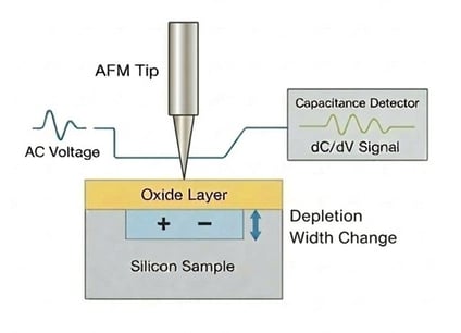
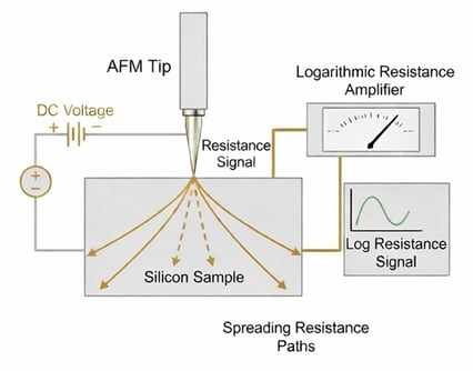
SCM SSRM
Applications
SCM
・Visualization of p–n junctions and doping polarity
・Electrical characterization of MOS structures
・Evaluation of low-doping-concentration regions
・Characterization of oxide/insulator interfaces
・Assessment of electrical inhomogeneity in nanodevices
SSRM
・Evaluation of high-doping-concentration regions
・Measurement of absolute carrier-concentration profiles (calibration sample is required)
・Analysis of leakage paths and abnormal conductive channels
・Characterization of wide-bandgap semiconductors (e.g., SiC, Ga2O3)
・Evaluation of contact resistance and interfacial conductivity
Features and Limitations
SCM
<Features> <Limitations>
| 1. | Can distinguish between n-type and p-type doping polarity | 1. | Absolute concentration evaluation is difficult (relative evaluation is possible) |
| 2. | Can visualize the p–n junction position with high spatial resolution | 2. | Signal tends to saturate in high-doping-concentration regions |
| 3. 4. |
Can detect low-doping-concentration regions with high sensitivity Can evaluate interfacial charges and electronic states |
3. 4. |
Sensitive to surface states and oxide layers Not suitable for analyzing current paths or leakage |
SSRM
<Features> <Limitations>
| 1. | Capable of quantitative carrier-concentration evaluation | 1. | Cannot distinguish doping polarity (n-type vs. p-type) |
| 2. | Strong performance in high-doping-concentration regions |
2. 3. |
Low sensitivity in low-doping-concentration regions Sample damage can occur due to probe contact |
| 3. 4. |
Can directly visualize leakage paths and conduction anomalies Applicable to wide-bandgap materials |
4. | Measurement results are strongly affected by cross-section polishing quality |
Important Notes When Making Analysis Requests
-Applicable to both SCM and SSRM-
Basic Sample Information
▸Sample size: from several mm to several cm (a size mountable on an AFM stage)
▸Sample thickness: a size of few hundred µm to few mm is desirable
▸Surface condition: a flat and clean surface
▸For cross-sectional observation: cross-section polishing is required
Required Information
▸Measurement objective (e.g., verification of doping profiles, identification of pn-junction locations, for failure analysis)
▸Information of sample structure (e.g., substrate material, layer configuration, device structure)
▸Measurement position, cross-sectional profile, measurement field of view
▸Doping elements and conductivity type (n-type / p-type)
▸Expected carrier concentration range