Features
-

Process Technologies Centered on Ion Implantation
We can accommodate a wide range of materials and needs, including various ion implantation techniques, film formation, and heat treatments up to high temperatures
-

Track Record in Handling New Materials (SiC、GaN、Ga2O3 etc.)
We accelerate R&D through a wealth of experience in handling new materials, new device development, simulation development, and various other semiconductor-related achievements
-

Broad Network Centered on Collaborative Research
We contribute to the advancement of semiconductors through a network involving numerous research and development institutions and external fabs.
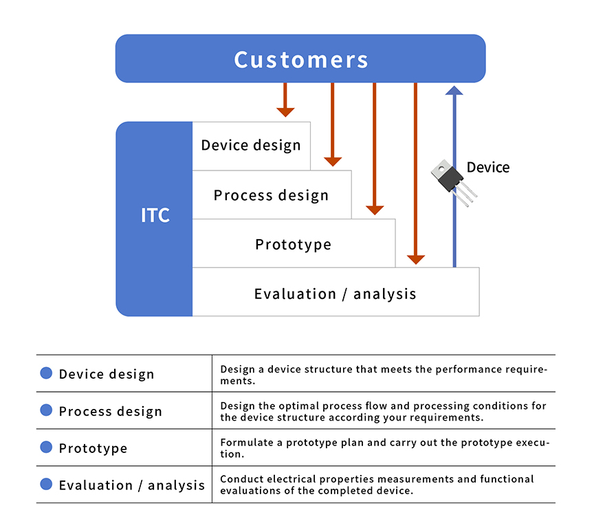
Capabilities of the Semiconductor Process Network
The Semiconductor Process Network offers flexible services tailored to budget constraints.
We will establish the environment necessary for prototyping, including design, processing, and evaluation. Utilizing this environment, we will coordinate the integrated prototyping and process prototyping of devices designed by the customer, and conduct evaluations.
We are willing to deal with small-scale, one-off projects. Above all, our commitment is to provide an empathetic, customer-focused approach.